Growth Strategy: Semiconductor Industry
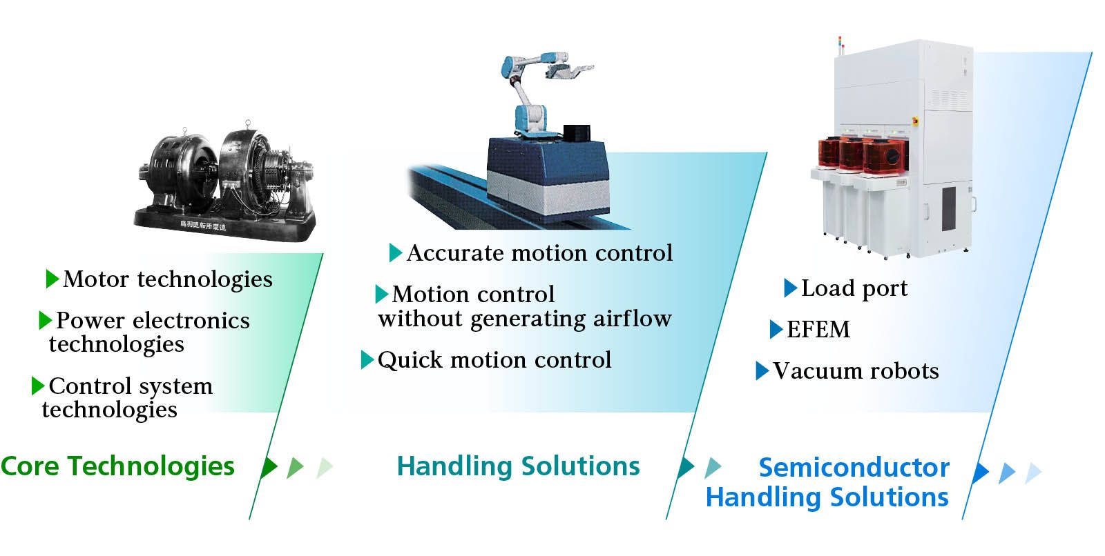
Applying Material Handling Solutions to Semiconductor Manufacturing Equipment
At semiconductor manufacturing facilities, even minute dust particles, slight vibrations, and marginal errors can significantly impact the quality of the semiconductors produced. SINFONIA’s advantage in the field of material handling solutions, which continues to allow us to support the semiconductor industry, is our ability to satisfy the stringent requirements of these environments.
Entry into the Semiconductor Equipment Industry
Since 1989, we have been marketing our material handling technologies to semiconductor facilities.
Since then, our material handling technologies have been widely adopted by the semiconductor industry and global market in overhead transport (OHT).
Since 1999, we have been evolving to meet the needs of our customers, capitalizing on our robotics technologies to expand into areas better described as manufacturing equipment, developing load ports and Equipment Front End Modules (EFEMs).
1989:
Delivered semiconductor manufacturing inter-process material handling systems (automatic guided vehicles [AGV] and overhead hoist transport [OHT])
Delivered vertical low-pressure CVD (chemical vapor deposition) equipment for semiconductor manufacturing
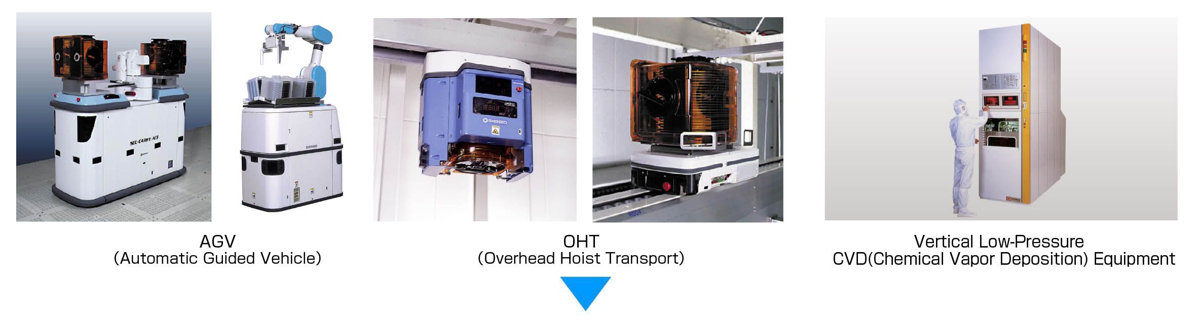
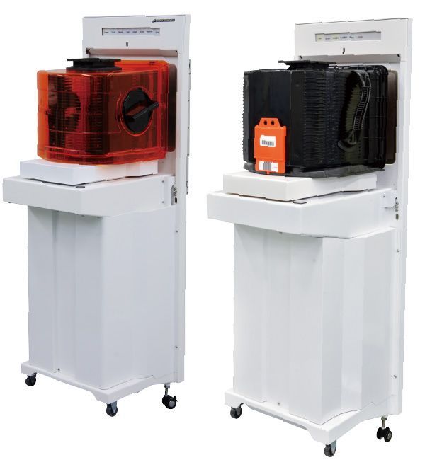
1998:Developed load ports and EFEMs

Left: Load Port, Right: EFEM
SINFONIA Products in Semiconductor Manufacturing Processes
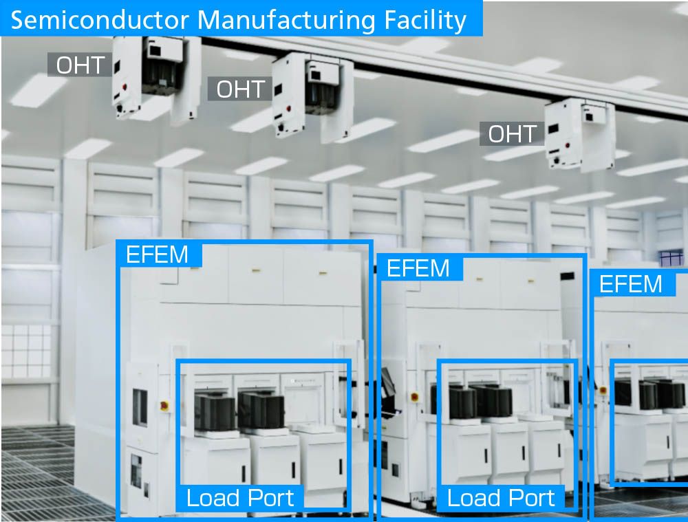
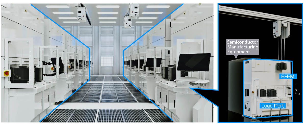
Semiconductor manufacturing is divided into front-end and back-end processes. In the front-end process, circuit patterns are created on silicon wafers, which serve as the building blocks of semiconductor devices.
Wafer processing encompasses a range of different sub-processes, each involving various items of manufacturing equipment.
It therefore involves transporting and transferring wafers between different pieces of equipment.
SINFONIA's material handling systems guarantee cleanliness and play a critical role in these handling and transfer tasks.
Our Semiconductor Manufacturing Technologies
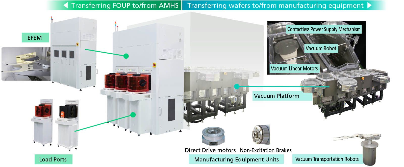
We possess a wide range of technologies that support semiconductor manufacturing. These include critical components such as load ports and EFEM, which are essential for loading and unloading wafers into and from manufacturing equipment.
We provide platforms and robots able to handle wafers in the vacuum chambers often used in semiconductor manufacturing.
We also supply direct drive motors, actuators, and electromagnetic brakes, which enable precise positioning of manufacturing equipment and control its operation.
Load Ports: World-Leading Market Share
Our load ports can be found in use in every area of the semiconductor manufacturing plant and boast the number one market share globally.
We are a leading supplier of one of the largest manufacturers of inspection equipment, known for its stringent quality standards. This recognition of our product quality offers us a competitive edge.
Future Outlook for the Semiconductor Manufacturing Equipment Market
With the advancement of AI, the IoT, and the Cloud, and the spread of EVs, we expect an explosive increase in demand for semiconductors by 2030.
As a result, we foresee significant growth in the semiconductor manufacturing equipment market, which will strongly influence sales in our semiconductor-related business.
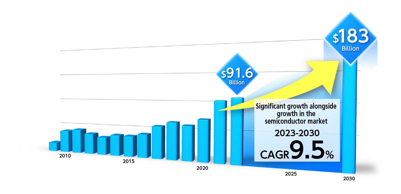
Source 1: Semiconductor manufacturing equipment market sales data based on Semiconductor Equipment and Materials International (SEMI) news releases.
Source 2: Compound average annual growth rate based on press releases from Global Information, Inc.
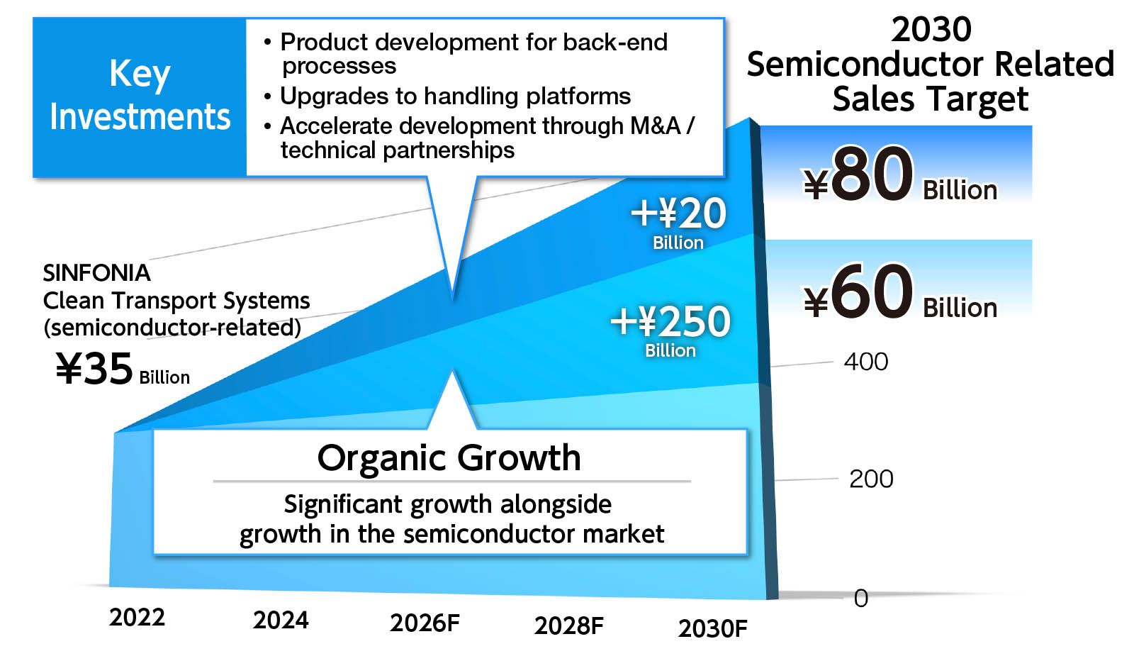
Future Goals for Our Semiconductor Business
In addition to organic growth driven by the expansion of the semiconductor market, we will focus on achieving sales of ¥80.0 billion in our semiconductor-related business by expanding and upgrading our lineup.
Future Product Development in Our Semiconductor Business
Further miniaturization is on the way in the front-end processes of semiconductor manufacturing.
We provide a wide range of products, including wafer handling systems suitable for use under normal atmospheric pressure and products enabling advanced environmental control such as nitrogen purging and use in vacuum.
To meet the increasingly advanced miniaturization needs of semiconductor manufacturing, we will accelerate our technological development, including of our next-generation load port , the Super Clean Load Port, and vacuum-compatible linear handling systems.
The demand for automation in back-end processes is also increasing.
We are enhancing our development and sales of products tailored to these new requirements, such as tape frame-compatible products and wafer level packaging (WLP) - and panel level packaging (PLP) - compatible products.
On the basis of the front-end handling expertise and technologies we can provide, we also participated in drafting the international standards for the Semiconductor Assembly Test Automation and Standardization Research Association.
We are contributing to the next generation of semiconductor manufacturing, including through the creation of uniform industry standards aimed at automation of back-end processes.

Tape Frame EFEM
")
Tape Frame FOUP Load Port(From left to right: SEMI E63, Taiwan & Korea Model, SEMI E184)
")
WLP/PLP FOUP-Compatible Load Port (SEMI Standards)
Expansion of Production and Improvement of Our R&D Structure
")
Expanding to Fab3, our new Clean Transport System factory (within Toyohashi Plant)
")
Our Clean Transport System factory (within Toyohashi Plant)
 Co., Ltd.)")
Expansion to the new Plant No. 3 (within Sinfonia Technology (Thailand) Co., Ltd.)
Our semiconductor wafer handling system products are currently produced principally at our Toyohashi Plant (Aichi Prefecture), along with our Ise Plant (Mie Prefecture) and Sinfonia Technology (Thailand). Anticipating future demand, we are continuing to expand these three plants as well as construct additional plants, in the aim of approximately doubling our current production capacity. Additionally, we have completed the acquisition of new land to prepare for further production capacity expansion.
In terms of our R&D structure, we are concentrating our technical resources on our semiconductor-related operations. In addition to establishing specialized departments aimed at establishing business in new semiconductor-related areas, we are actively building cooperative relationships with customers and suppliers.

Quick Overview of SINFONIA
Growth Strategy: Semiconductor Industry
Growth Strategy: Aerospace Industry